|
Facilities |
||||||||
|
|
|
|
|
|
|
|||
|
|
UCSB
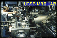
NanoFabrication Facility MBE Lab: Our III-V device research relies on the collaboration and efforts of our colleagues in the UCSB MBE lab. This is one of the worlds' largest academic laboratories for research in semiconductor materials and semiconductor growth. MOCVD Lab: Home to 5 MOCVD
and 3 HVPE systems for growth of GaN and related materials, InP materials for
photonics and high-speed electronics, and semiconducting oxides. MOCVD is
critical for regrowths in advanced high-speed transistors High Speed
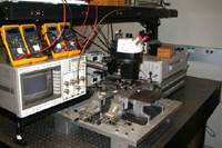
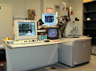
Electronics Lab: (Rodwell & Buckwalter lab) This is a design and test facility. We have computers for design using both III-V (Agilent ADS) and VLSI-centric (Cadence) design tools. Our network analyzer, probe stations, and probes provide measurements from DC-330 GHz. Our digital test station provides clock signals up to 210 GHz, and can measure signal spectra to 330 GHz and waveforms to 110 GHz. Microscopy and Microanalysis
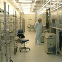
Facility This lab,
part of the Materials Research Laboratory in the UCSB Materials Department,
offers advanced advanced tools for device and materials analysis.
Capabilities include TEM, SEM, SFM/AFM, SIMS, FIB/SEM |
|
||||||
|
|
||||||||
|
University of California, Santa
Barbara Department of Electrical &
Computer Engineering University of California, Santa
Barbara, CA, 93106 |
||||||||