Schematic illustrating
my future work which will be dedicated to interdisciplinary research
relating to III-V compound semiconductor materials and devices that
bridges engineering, optics, applied physics and nanoscience or
nanotechnology.
Current Research
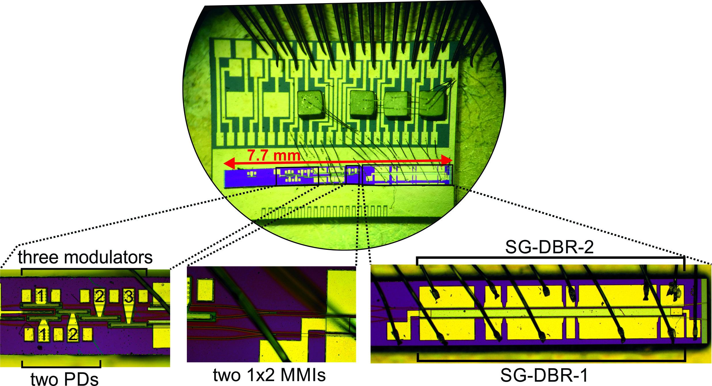
My current research in UCSB, CA, is primarily
focused on the growth, design, fabrication and characterization of InP-based
photonic integrated circuits, in particular, on-chip optical frequency synthesizer
(OFS) using optical phase-locked loop (OPLL).
My research interests and expertise
lie in:
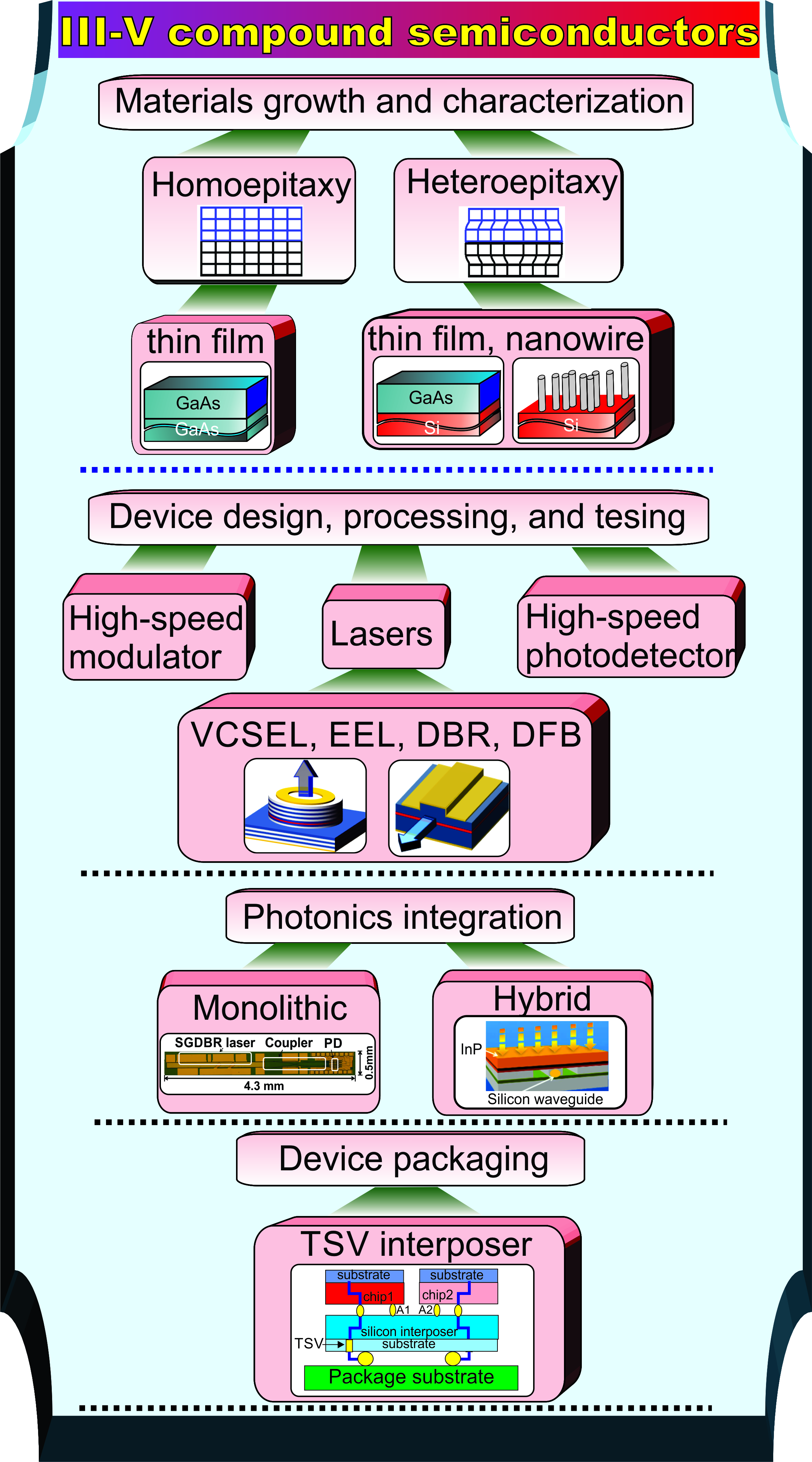
 Semiconductor Lasers, e.g. DFB, VCSELs, coupled-cavity lasers
Molecular Beam Epitaxy, e.g. homo- and heteroepitaxy-based thin film,
nanowire
Nanophotonics, e.g. Nanocavity LEDs, Lasers
InP-based Photonic Integrated Circuits
Graphene Photonics
Silicon Photonics
PIC on
TSV interposer
Postdoctoral Research at McGill
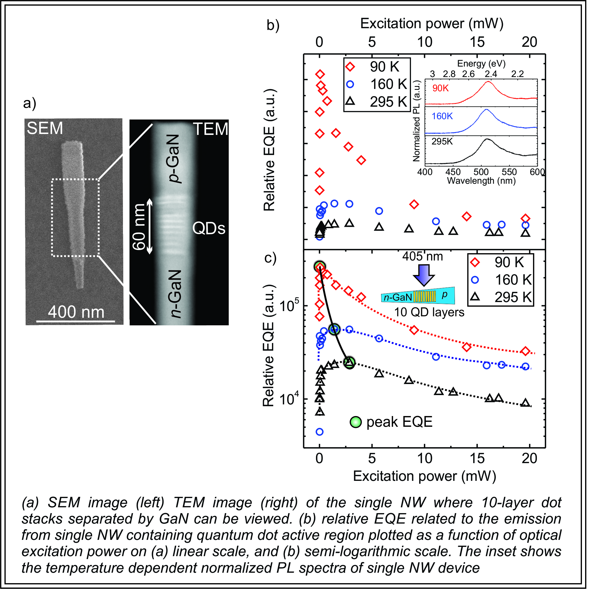
While at McGill, my research was
focused on the detailed optical and electrical characterization of
III-nitride (AlGaInN) single nanowires. As it is known that 1D
nanostructures, such as nanowires and nanorods, based on the III-nitride
materials system have attracted attention as potential nanoscale building
blocks in light emitting diodes (LEDs), lasers, sensors, photovoltaics, and
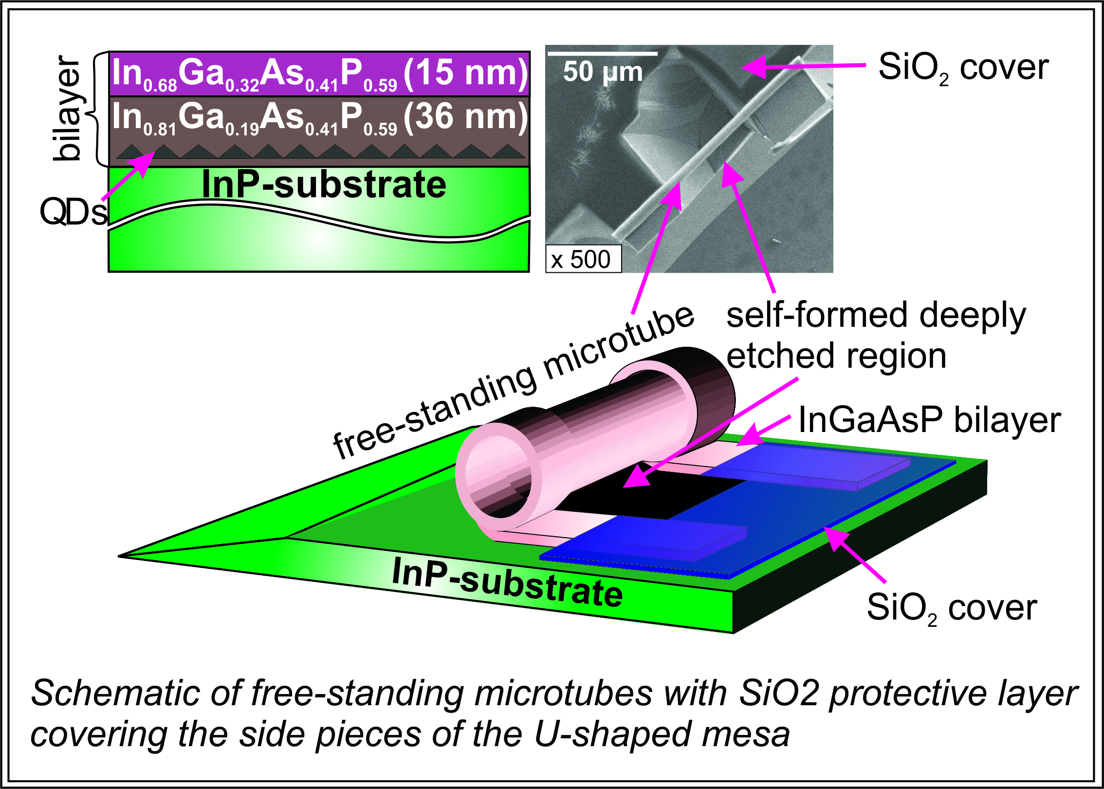
high power and high speed electronics. Furthermore, I worked on the
fabrication and optical performance of micro- and nanoscale quantum dot tube
structures that are expected to emerge as novel building blocks for
high-performing nanophotonic devices.
Postdoctoral Research at UCLA
While at
UCLA,
My research was focused on
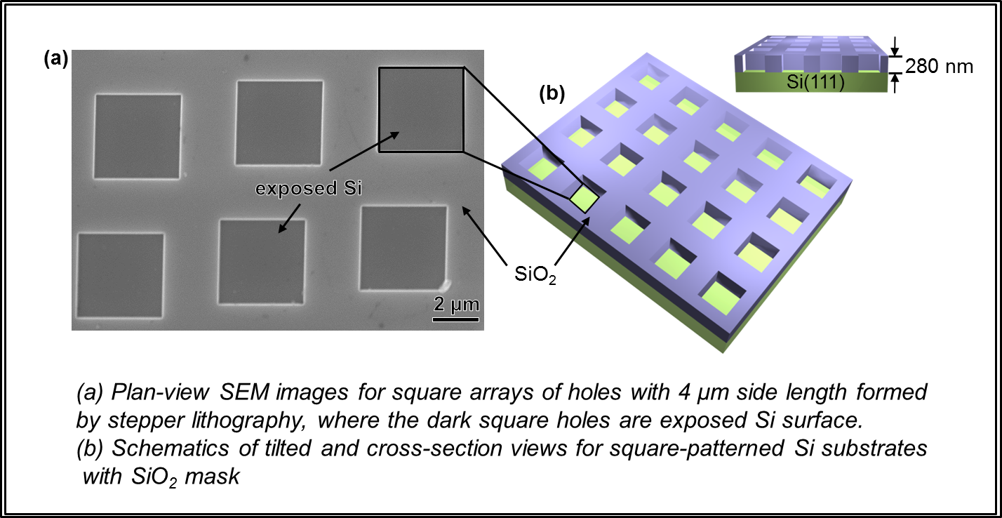
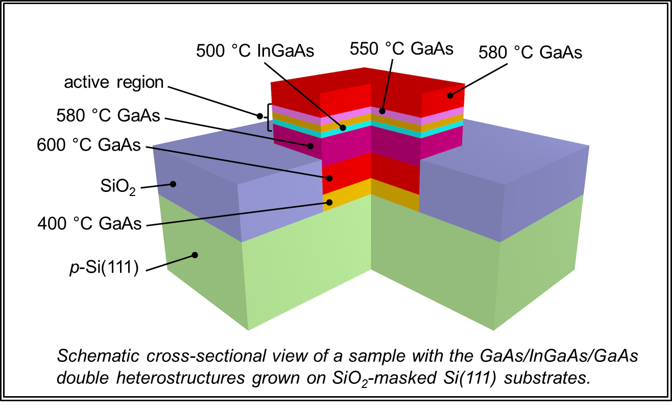
o Patterned
growth of GaAs films on silicon substrates : growth of high-quality and
defect-free GaAs by molecular beam epitaxy on silicon dioxide patterned
Silicon(111) substrates for building active optical devices including light
emitting diodes, lasers and photodetectors on Si, making it a remarkable
step towards an eventual demonstration of the microelectronic and
optoelectronic devices on the same chip.
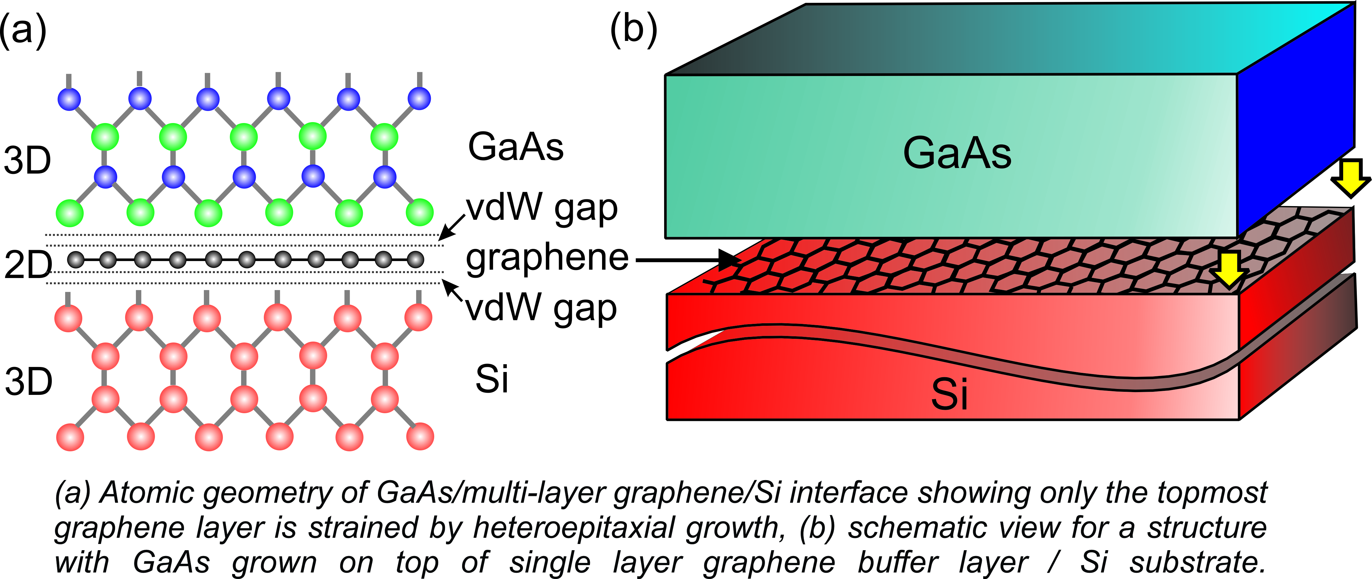
o Van der Waals epitaxial
growth of GaAs thin films on silicon using a twodimensional layered
material, graphene as a lattice-mismatch and thermal expansion coefficient
mismatch-relieving buffer layer : a potential route towards heteroepitaxial
integration of GaAs on silicon in the developing field of silicon photonics.
On the way towards its realization, a deposition of high-quality GaAs films
on graphene/silicon by molecular beam epitaxy and then a detailed material
characterization are required.
o Graphene
as transparent electrode for GaAs-based vertical-cavity surface-emitting lasers:
the graphene material-based electrode in VCSELs can bring three benefits: a
reduced lateral resistance of the laser leading to an enhanced frequency
modulation response and reducing the series resistance leading to an improved
thermal characteristic.
PhD research
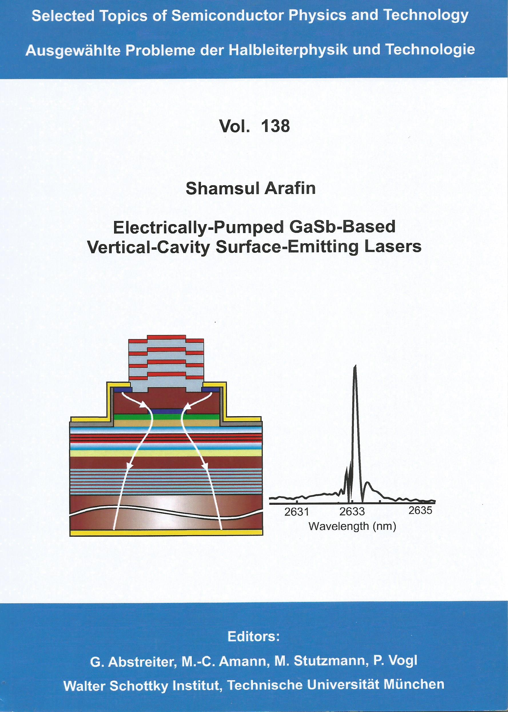
My PhD thesis was focused on the development of novel electrically-pumped
(EP) continuous-wave (CW) operating GaSb-based application-suited VCSELs in
the wavelength range between 2.3 µm and 2.6 µm. In particular, much emphasis
was laid on devices with record long emission wavelengths of 2.6 µm which
exhibit single-mode operation with a reasonably wide mod-hop free tuning
range. The design, fabrication and especially the characterization of such
lasers were performed during the thesis. This thesis also presented some
design principles for next generation high performance GaSb-VCSELs based on
the device characterization results. The examination of the several
individual components of the device and their successful implementation onto
the device are also covered here.
Citation of my PhD thesis (book)
Shamsul Arafin,
Electrically-Pumped GaSb-Based Vertical-Cavity Surface-Emitting Lasers,
Selected Topics of Semiconductor Physics and Technology, vol. 138,
Walter Schottky Institut, Garching, Germany, 2011. 136 pages. (ISBN
978-3-941650-38-1)
MSc research
My M.Sc. thesis was focused on
the investigation into matrix addressable VCSEL array fabrication and the
characterization afterwards. Recently this matrix addressable array has got
great importance due to plenty of attractive applications like confocal
microscopy, non-mechanical particle movement by optical tweezers, and video
imaging where a large number of parallel optical sources with desired beam
profile are needed. Matrix addressable VCSEL array can be the strong
candidate to be implemented in these demanding applications since matrix
addressing technique is capable of producing larger and denser 2-D array
easily than independent. The entire work was performed on the sample
designed for the standard wavelength regime around 850 nm, grown by solid
source molecular beam epitaxy (MBE) on undoped GaAs substrate.
Citation of my MSc thesis
Shamsul Arafin,
Invetigations
into Matrix Addressable GaAs-VCSEL Arrays,
M.Sc. Thesis, University Ulm, Germany, 2008. 126 pages.