Bowers "The Power of Light-driven Computing"
The U.S. is winning a global battle for domination in integrated photonics and manufacturers embracing AI and ML will benefit, according to ECE Prof. & Acting CEO of AIM Photonics, John Bowers
"AIM Photonics will give already-exploding AI/ML shot in the arm"
Excerpt from the Smart Manufacturing magazine article
This is thanks in part to The American Institute for Manufacturing Integrated Photonics (AIM), a Manufacturing USA innovation institute that the Obama administration stood up in 2014.
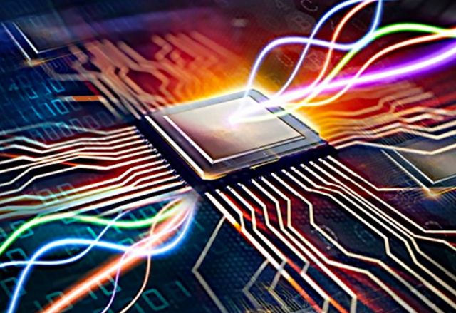
“The chips that Intel and Broadcom announced recently are 25-terabyte-per-second chips, so that’s 25,000 gigabytes/second, or 25 million megabytes/second,” John Bowers said. “That’s how much data each of them processes. It lets your networks just keep getting faster and more complex, so they can handle more data.
“Where that really matters is for things that involve AI and machine learning (ML). They take huge amounts of computing capacity,” he said. “And for data centers to be able to handle that, they need this much higher capacity,” which is partly due to the fact that capacity of an optical fiber is 1,000 times that of an electrical wire, and that the signal loss in fiber optics is “about 1,000 times lower than electrical wires.”
To get to the point of building terabyte chips alongside industry partners like Intel and Broadcom, AIM Photonics has played a leading role in three dramatic shifts in the making of microchips.
First, researchers at U.C. Santa Barbara (UCSB), an AIM Photonics member, working with Intel made history when they “developed the technology to integrate lasers onto photonic integrated circuits (PICs),” Bowers said. UCSB then teamed up with Intel to integrate lasers onto PICs. “Intel is now making photonic integrated circuits.”
Second, the institute is challenging the norm of making PICs using materials like indium phosphide or gallium arsenide or gallium nitride. “They’re so-called III-V materials, meaning column three, column five of the periodic table. And those materials are very efficient light emitters,” he said.
“The photonic integrated circuit industry has been entirely based on indium phosphide and these III-V materials” but researchers at AIM Photonics are leading the switch to silicon, he added.
To be sure, there are “big efforts” to do the same—which means making photonic integrated circuits in a fully automated CMOS (complementary metal oxide semiconductor) foundry—in Asia and Europe, including at AI specialist IMEC, Bowers said. “It’s a global race. And I would say Intel is leading the commercial end of it, and AIM is leading the research end of it.”
One of AIM’s central goals is “to make photonic integrated circuits the same way electronic-integrated circuits are made,” he said.
On this front, Taiwan Semiconductor Manufacturing Co is nibbling at Intel’s heels.
It is exactly the sort of situation U.S. President Joe Biden spoke to in 2014 as he announced the formation of AIM Photonics: Then-Vice President Biden noted that the U.S. used to lead in photonics and telecommunications—but that after 2000 there was a big collapse and much of the manufacturing for photonics got sent to Asia because it was very labor-intensive, Bowers recalled. “The decision was made to have an institute in integrated photonic circuits” in order to leapfrog similar efforts around the world.
“We now have a photonic design capability that is No. 1 in the world,” he asserted. “The whole effort has been transformative.”
Intel is now making photonic integrated circuits. “I would say, in terms of doing this on silicon, they’re the world leader,” Bowers said. Other than Intel, “no one really integrates all the photonic elements on silicon, including the laser,” he added. “The laser is typically off chip because integrating it is a difficult problem to solve.
AIM Photonics has what he called “a major new research effort” to integrate all the photonic elements on silicon. It is a collaboration between UCSB, a company called Analog Photonics and SUNY (State University of New York), which hosts the institute. The PICs are made in a CMOS-foundry-like R&D center called Albany Nanotech, and after the chip wafers are diced up, the chips are packaged in Rochester. Analog Photonics leads the photonic design kit (PDK). UCSB’s Institute for Energy Efficiency is the West Coast headquarters of AIM Photonics.
Engineers use an X-ray fluorescence tool to analyze wafers in AIM’s test, assembly and packaging (TAP) facility in Rochester, N.Y.
The third dramatic microchip-making shift in which AIM Photonics has figured prominently is in 3D-bonding optics with electronics. “That means that the input and the output on electronic chips can now be optical”—which increases the speed and capacity of data transfer and reduces the power required to do so, Bowers said.
“Before long, your processor in your computer will be communicating with other chips in your computer optically,” he added. “That is a huge revolution. What that really drives is silicon photonics. Because now you need to be doing everything on silicon since the chips all need to have the same expansion coefficient.”
The imminent switch to photonic communications will mean products as ubiquitous as the personal computer will change dramatically.
“The optical connection is going to go all the way to the processor in your computer,” Bowers said. “Today, you connect up to this electrical Ethernet cable or wi-fi connection. But in the future, inside your computer, it’s going to be optical. And that’s as big a revolution as the whole Internet was: Internet and fiber optics together. That would have never happened unless we had high-capacity connections.”
When the chip is co-packaged, “the data going in and out of that chip” will no longer be electrical, he said. “Today, every processor chip, memory chip, switching chip, FPGA chip you buy, all have electronic I/O, input and output, and that is going to change.”
Read more in the full article about:
- Funding Comes from all Corners
- Impact to Be Felt First in Automotive, Medical Fields
Smart Manufacturing magazine – "AIM Photonics will give already-exploding AI/ML shot in the arm" (full article)
by Brett Brune, Editor in Chief, Smart Manufacturing magazine