J. Jiang – ECE Outstanding PhD Dissertation Award
Junkai Jiang recently receives his 2020 award from the ECE Department – doctoral students who received their Ph.D. degree from Fall 2019 to Fall 2020 were considered for the award based on their faculty advisor’s nomination
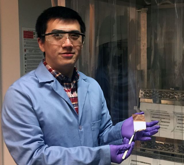
Junkai’s dissertation titled "CMOS-compatible doped-multilayer-graphene for next-generation interconnects, passives, and monolithic-3D ICs," focused on the applications of the two-dimensional (2D) material - graphene, as on-chip interconnect and passive devices, as well as in monolithic 3D integration. It experimentally demonstrated a novel pressure-assisted solid-phase diffusion synthesis method, which is the only low-temperature and transfer-free synthesis method among the reported ones (IEDM 2018). It also developed a unique graphene doping method by intercalation using a custom-designed and fabricated high-pressure reactor (Nano Letters 2017). A multi-level graphene interconnect scheme with vertical via connections was also demonstrated displaying superior performance and reliability compared with conventional metal interconnects (IEDM 2017). The doped graphene interconnects demonstrated in this dissertation overcame a major challenge in today’s back-end-of-line metal interconnect technology, in terms of performance, energy-efficiency and reliability – The UCSB Current "Graphene Goes Mainstream". The graphene interconnect technology offers a promising solution to semiconductor technology scaling towards sub-5 nm nodes, and thereby sustain Moore’s law. This dissertation also helped solve a long-standing problem in graphene research by demonstrating a large-area, low-temperature, and transfer-free graphene synthesis method that offers high-quality multilayer graphene directly grown on dielectric surfaces. This CMOS-compatible graphene synthesis technology has been highlighted by Nature Electronics and the IEEE Electron Devices Society Newsletter, and also reported by Wikipedia. The intercalation doping technique and the corresponding theoretical understanding of intercalated graphene also paved the way for the demonstration of highest inductance density materials ever made by exploiting kinetic inductance at room temperature for the first time (Nature Electronics 2018). This has opened new opportunities in inductor scaling that is critical for miniaturization of IoT devices and energy-efficient design of power delivery systems. This work has been highlighted by top international media websites, including Forbes and PhysicsWorld. Finally, this dissertation revealed that Moore’s law can be extended well beyond the foreseeable roadmap of transistor scaling and unprecedented beyond-Moore heterogeneous integration can be realized by monolithic integration of 2D materials in 3D ICs – The UCSB Current "Saving Moore’s Law."
Junkai Jiang was born in Nanchang, Jiangxi Province, China. He received the B.Sc. degree in microelectronics from Peking University, Beijing, China, in 2012. In Fall 2012, he joined the Nanoelectronics Research Lab (NRL) in the Electrical and Computer Engineering Department, University of California Santa Barbara as a MS/PhD student under the tutelage of Prof. Kaustav Banerjee. His research focused on the modeling, design, and fabrication of emerging interconnect structures and passive devices based on graphene and other 2D materials, earning him the Ph.D. degree in 2019. Junkai’s doctoral research has been recognized with the IEEE Electron Devices Society’s PhD Fellowship Award (2018) and UCSB's Winifred and Louis Lancaster Dissertation Award (2020) that was highlighted in The UCSB Current article "Significant Impact." He also received the Best Student Paper Award at the 2018 IEEE S3S Conference. He is currently an R&D engineer at Google in Sunnyvale, CA, USA.
The ECE Outstanding PhD Dissertation Award includes a $1,000 stipend and a memento in recognition of the accomplishment.