COE Convergence (S23): "The Nanofab"
The Nanofabrication Facility is where researchers in “bunny” suits transform exotic materials into advanced electronics for academics and industry
- From the COE/CLS Convergence (S23) magazine article "Tech Edge: The Nanofabrication Facility"
- Check out the COE "In Focus" video "The Nanofab: An Innovation Center"
Matthew Wong, a UC Santa Barbara assistant project scientist who earned his PhD with UC Santa Barbara professors Shuji Nakamura and Steven DenBaars, visited numerous cleanrooms recently while traveling the country to interview for faculty positions. Someone who worked at one of them and learned where Wong was from said to him, “The UCSB facility is like the Holy Grail of cleanrooms.”
“In the global semiconductor community, UCSB is known in part for the Nanofab and the activities it supports,” says electrical and computer engineering professor and Nanofab director, Jonathan Klamkin. “When prospective faculty interview and are asked why they are interested in UCSB, one of the more popular answers is ‘the Nanofab.’”
The lab plays a key role locally and regionally in what the facility’s technical and operations manager, Brian Thibeault, describes as a key “second part” of the semiconductor industry.
“There‘s the silicon industry, which supplies all the microelectronics and the computational stuff we have,” he says, “but then there’s a whole other semiconductor industry that produces many things — the devices that produce light, or RF [radio frequency] power out of your cell phone, or do the facial recognition on it. And it’s all the other semiconductor materials developed at this university and others that make advancements in electronics, optics, and such possible. The bread and butter of our lab lies primarily in that ‘beyond silicon’ world.”
Open 24/7 and often booked 16 to 18 hours a day for weeks on end, the lab sees some 6,000 to 7,000 billable hours of use per month. Industrial users — from small local startups to giants like Google, which has a team here doing development work on the chip for a quantum computer — account for about 55 percent of the total.
“We have a substantial industrial user base, and slightly over half of the more than 500 annual Nanofab users are employed by fifty-plus companies,” Klamkin says. “Having industrial and academic users working in the same facility fosters a highly collaborative ecosystem that facilitates ‘lab-to-fab’ transitions. The Nanofab plays a critical economic role both locally and more broadly.”
“It’s a user-fee-based operation,” Thibeault says, noting that the roughly 12,000-square-foot space, most of which is occupied by the cleanroom, has an annual budget of about $6 million and a staff of about 20. “Those billable hours keep the lab running and allow us to reinvest to keep improving it and keep it relevant and state of the art.”
The Nanofab is also heavily used by UCSB researchers. Thibeault once did a study with the UCSB Office of Research and discovered that researchers on some 35 percent of all grants at UCSB used the facility in some way.
Nanofab leadership has also recently replied to solicitations for funds from the $50 billion-plus CHIPS and Science Act of 2022, aimed at strengthening the U.S. position in semiconductor R&D and manufacturing. As part of that effort, Klamkin notes, “We’ve had visits from our district Congressional representative and from the Deputy Secretary of the Department of Commerce.”
Read more of this article and the Nanofab in the accordions below:
- Small, Complex, Precise
-
Small, Complex, Precise
Describing Nanofab work in the simplest possible terms, Wong says, “You either remove material by etching or use a deposition to add relief. You add something or you take something off. That’s basically what a cleanroom is.”
It is, of course, the details within that easy description, reflected in dozens of related processes, the tiny scale at which they unfold, and the exacting precision with which they must be performed that makes this kind of “simple” adding and subtracting of materials Nanofab-dependent.
For his graduate research, Wong worked to eliminate an inefficiency in micro-LEDs, which he calls “the next generation of display technology.” The lights are tiny, as their name suggests, and the semiconductor’s light-emitting layer is susceptible to being damaged during fabrication, thereby reducing efficiency. “You define the lighting area, which has a diameter smaller than that of a human hair, by etching with plasma to remove materials,” he explains. “Plasma etching works by placing a material sample between two plates and flowing gasses into the area. When a voltage difference is applied between the plates, the gas is ionized and hits the sample, performing the etching action.” In his research, Wong employed different methods — and has developed recipes for them — to mitigate the effects of that damage and, thus, recover the efficiency of the micro-LED.
Nanofab work is all about scale, which is why everything needs to be so clean, and why users wear protective white “bunny” suits. “My work requires an environment largely free of particles to eliminate any chance of contamination, which can cause irregularities and variations on the wafer,” Wong says. “At the micron scale, there is not much room for error.”
- Layout and Process
-
Layout and Process
The cleanroom is arranged into seven rows, or bays, each about fifty feet long and equipped with tools and benches to support tasks related to specific processes. There are two lithography bays, each bathed in amber light, where the critical step of patterning on wafers occurs.
“Patterning is the heart of fabrication; it’s how you implement your idea,” Thibeault says. “We have people here who do this incredible high-end research for product development where they're patterning at the 10-nanometer scale or below. So, you might need electrons to come over here and photons to come out over here, and you need to have the shapes like so and arranged this way to work according to your mathematics. The more precision and quality you can bring to performing those steps, the more likely you are to implement your ideas.”
Getting the pattern onto the wafer involves a series of steps that often start with cleaning to help with adhesion. This can be done using solvent or an oxygen-plasma process, or sometimes, a stop in the “acid bay” is more appropriate. “Brand-new wafers are pretty clean when they arrive from the vendor, but some processes require additional cleaning before the wafers are used,” says Paula Heu, who has spent over a decade doing process development in the Nanofab for industry users. “Some materials have a native oxide that grows naturally, and certain electrical contacts require that the interface between them have no oxide. Specific acids are then used to strip off the native oxide before depositing metal.”
"Every imperfection may add to the ‘loss’ of the laser cavity and a ect performance. Sometimes in our work, we’re looking for the laser to have record-breaking performance, and for that you need everything to be perfect."
Next door, the lithography bay includes “spin stations” for coating wafers with a photo-sensitive resist material. The lab has numerous ovens and hotplates for curing photoresist and for thermal processing of photolithography, as well as ionbeam and electron-beam lithography systems and stepper tools for exposing patterns at extremely high resolution.
During lithography, Heu explains, “a pattern is transferred onto a wafer by coating it with photoresist, exposing the photoresist to UV light through a mask, and then developing the photoresist. You then rinse it off and inspect it, with the pattern now transferred onto your wafer.”
Next, the wafer is inspected using either an optical microscope or one of the lab’s two scanning electron microscopes (SEMs), depending on the resolution needed, “basically to see if what you have intended to pattern looks good and is sharp,” Heu says. “The first round is to see where you are in your process, and then you can fine-tune it so that it will allow you always to get a good result.”
Once the pattern has been transferred to the wafer, the process moves to fabrication, which involves a series of steps. They may include wet or dry etching to remove material, using one of the deposition tools to add material, or plasma treatments, high-temperature baking, or annealing to achieve high-temperature bonding of metals. Kaiyin Feng, a sixth-year PhD student in the lab of John Bowers (Materials, Electrical and Computer Engineering) who focuses on high-performance lasers used in photonic integrated circuits (PICs), spends much of her time in the Nanofab working on process development and fabrication of prototypes of novel devices.
Using material grown by students or postdoctoral researchers in the Bowers group, she says, “We design single device components or sometimes a photonic circuit on-chip. That might be a novel laser or a tiny circuit, such as a laser connected to a waveguide that splits the light into two pathways for different downstream functionalities.”
The work of building such nanoscale structures could not be done without the Nanofab.
“After the design is done, we also need to figure out how to make them,” Feng says. “For example, we have to figure out which lithography recipe suits the patterning resolution, which chemistry gives the best etched sidewall, or what metal alloy gives the lowest contact resistance. There’s a lot of chemistry and materials engineering happening, and sometimes, as process development, we need to do a few short iterations to figure out the recipe for one step. The Nanofab serves as a perfect environment for us to perform these experiments. After resolving all the challenges in each step of the fabrication process, we can actually make the device we designed!”
Evaluating results through observation and measurement — the entire metrology bay is filled with nothing but precision-measuring tools — is a time-consuming but critical part of both lithography and fabrication. “You might spend two hours using the SEM to check every detail of a step to make sure the fabrication went correctly,” Feng says. “You’re completing the process, because if something is a little dirty, it will affect all the following [fabrication] steps, so you have to clean it up. It might be some hardened polymer from the dry etch that sticks to the wafer, so you use different chemicals or different cleaning plasmas to remove it, and then you keep checking to see if it’s clean. Every imperfection may add to the ‘loss’ of the laser cavity and affect performance. Sometimes in our work, we’re looking for the laser to have record-breaking performance, and for that you need everything to be perfect.”
Talk to any Nanofab user, and especially long-term users, and they’ll mention the incredibly helpful staff that makes the place work. “They do such a good job maintaining the tools, so that we don’t have to fix them ourselves as students,” Feng says. “We work 24/7 on a flexible schedule, and sometimes they are on call for emergencies late at night or during the weekend or on public holidays. That’s really helpful when you’re stuck in the middle of something and trying to figure out what’s wrong with a tool.”
The staff includes a team of process and equipment engineers who calibrate the various tools every week to ensure that they are within specifications. “That way,” Heu says, “if your process results are unsatisfactory, maybe after lithography, you know that it’s not an issue with the tool. The process people make sure that you get a repeatable result time after time.”
In the Nanofab, it’s always the (very) small things that matter most.
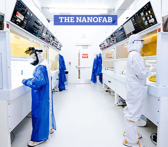
Image Caption: In the acid bay, researchers and technicians clean wafers before or after various processes to eliminate particle contamination and material imperfections that can affect the final product.
COE/CLS Convergence magazine (S23) - "Tech Edge: The Nanofabrication Facility"