Emmanuel Kayede – MS/PhD student in Electronics & Photonics
In his own words – Interviewed during 3rd year (Summer 2020)
- Hometown: Los Angeles, CA
- Previous Degrees: BS degree in Electrical Engineering from the University of California, Santa Cruz
- Degree Sought from UCSB: MS/PhD, 3rd year
- Advisor / Lab: Umesh Mishra
- Research Program: Electronics and Photonics
- Main Area of Research: Nitrogen polar gallium nitride (N-polar GaN) high electron mobility transistor (HEMT)
- Research Interests: N-polar GaN HEMT, 1/f Noise
- Important Conferences: I gave a talk at Electronic Materials Conference, Virtual 2020
- Important Awards & Honors: Bridge to Doctorate and Honorable Mention Graduate Research Fellowship
- UCSB Student Organizations: Society for the Advancement of Chicanos/Hispanics and Native Americans in Science
- Professional Memberships: Materials Research Society (MRS), National Society of Black Engineers (NSBE)
- Hobbies and Interests: Rock climbing, hiking, mountain biking, photography, playing the guitar
Favorite things about
- Department: The spirit of collaboration between departments (Materials, Bioengineering, etc) at UCSB and outside of UCSB.
- UCSB: Due to the proximity of the beach to our office, my lab mates and I are able to take short mental health breaks at the beach. I also appreciate the vast opportunities for mentoring and professional development at UCSB.
- Santa Barbara: Outdoor recreational activities like hiking, rock climbing, mountain biking, swimming in the ocean, and many more!
Emmanuel and his research
Tell us about your research
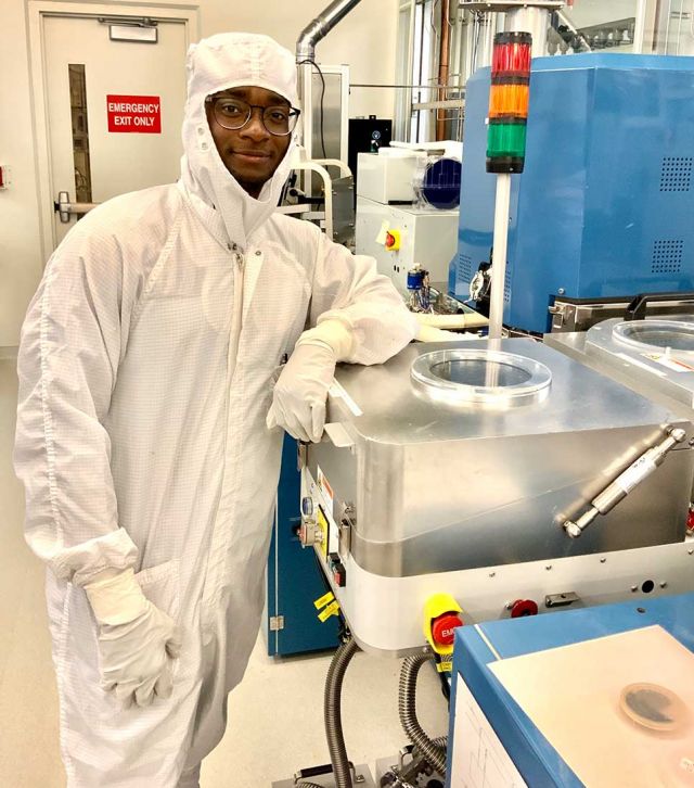
My research is on developing highly efficient Nitrogen-polar GaN HEMTs for use in solid-state millimeter-wave power amplifiers. This device technology has demonstrated significant performance advantages over traditional Ga-polar GaN devices and still has many unexplored properties. One of these properties is that the surface is more chemically reactive relative to Ga-polar GaN. In my research I am exploiting this property to identify wet-etchants to develop low-cost manufacturing processes while also further improving the device performance. On a daily basis, my research involves patterning N-polar GaN samples by photolithography, wet etching these samples, and examining the surface of the substrates using scanning electron microscopy and atomic force microscopy.
How and why did you get into your area of research?
Through the University of California's Leadership Excellence through Advanced DegreeS (UCLEADS) and UCSB’s Materials Research Institute Future Leaders in Advanced Materials (FLAM) summer research internship, I was able to intern at Professor Mark Rodwell’s High Speed Electronics Group here at UCSB. These internships shaped my passion for transistor design and fabrication. When I arrived at graduate school, I wanted to explore a different material system (GaN). After sharing my interest, my advisor happily gave me a research project.
Why did you select UCSB and ECE in regards to your research?:
The ECE department has established itself as a leading research institute in the fields of III-V technology. UCSB also has an amazing cleanroom facility (UCSB Nanofab) which consistently works with graduate students to develop devices for their Masters and PhD thesis. Furthermore, having interned at UCSB prior to graduate school I knew I could rely on a support network, namely Val de Veyra, the graduate student affairs manager, and my fellowship program (Bridges to the Doctorate Program).
What do you find rewarding about your research?
The relevance of my research for developing wireless communication systems (like 5G), radar transmitting technology (like LiDAR), and high-resolution imaging systems for autonomous vehicles and ultraviolet detectors.
UCSB prides itself on its collaborative atmosphere, give some examples of how you collaborate
I am fortunate to be able to collaborate with my lab mates who grow high-quality GaN materials for my research. In addition, my research group is part of the Communication, Sensing, Terahertz (ComSenTer) Center, a collaboration between three UC campuses and other institutes working to develop wireless communication systems. We collaborate with Professor Elaheh Ahmadi at University of Michigan, Teledyne, and several other professors both at UCSB and elsewhere.
What's it like working in a group research environment and your experience working with an advisor?
My research group is split into two teams, materials growth and device design/fabrication. With two teams the work of developing transistors from epitaxial growth to device design and fabrication is made easier, fostering a work culture that is both collaborative and supportive. This of course would not be feasible without a capable advisor, who is both somewhat hands-off, yet still very approachable and supportive.
Academics at UCSB
Strengths of the graduate program
In all of the courses that I have taken, the professors have been very accessible and available. The coursework is interdisciplinary, and students from different departments enroll in classes. With this in mind, the lessons often include applications and perspectives from multiple areas of studies.
Favorite course
Device Physics (ECE 221A) taught by Professor Mishra. The class is on the fundamentals of semiconductor devices. The class assignments and exams often include problems that have been encountered in research. So, cookie-cutter solutions are not applicable to these problems. However, Professor Mishra’s lectures are structured in such a way that helps students develop an intuition for solving new and challenging problems both during and outside of the class. Moreover, because of the fascinating life experiences shared by Professor Mishra, there is rarely a dull moment during lecture.
Life as a graduate student
Quality of life as a graduate student and how you balance school, work, social, and family life
Finding a balance in graduate school takes practice and effort. I strive for a 9-5 work schedule, which allows me to spend time on my social and family life. I also like to end my workday with a workout; going to the gym or going rock climbing at the end of the day helps me relax. While I like to work on a 9-5 schedule, my schedule is still flexible because I have to schedule my time around cleanroom equipment access. In general, finding a balance in graduate school requires effort but I like to think it is essential for a successful and happy graduate career.
What is your social life like and where have you lived?
I have close friends in my department and in other departments. I also try to make new friends outside of UCSB. My friend group outside of academia helps me connect with the rest of the world and escape the academia bubble. While housing in Santa Barbara can be expensive, the grad student housing (San Clemente) is very budget friendly. I currently live at San Clemente, but I will be relocating to Goleta to get a better sense of the feel of the town.
What do you plan on doing over the summer break?
Next summer, I plan on working on my research and visiting national parks that I have yet to visit.
Advice to prospective graduate students
Don’t hesitate to ask for help, make friends in and out of your department, and take your time in choosing an advisor and a research group.
Future Plans...
Do you plan to go into academia or industry?
While I do not have definite plans at the moment, I would like to take the industry route after graduation.