ECE Research Initiative
John Bowers | "Convergence of Silicon Photonics and Electronics"
From The ECE Current Newsletter (Fall 2021)
Modern CMOS packaging techniques, including those originally developed for the cell phone and IT industries, are being applied to silicon photonic integrated circuits (PICs), resulting in much lower costs and far improved scalability
Silicon photonics research and commercialization has intensified as both photonic component performance and photonic integration complexity have been dramatically improved and expanded in the past decade. Silicon photonics enables a wide range of applications from datacom and telecom to sensors including light detection and ranging (LIDAR), gyroscopes, biosensors, and spectrometers. The key drivers for using silicon for photonics include the advantages of low-loss silicon waveguides with compact size and excellent uniformity, resulting from the high quality and mature processing of CMOS processing. Modern CMOS packaging techniques, including those originally developed for the cell phone and IT industries, are being applied to silicon photonic integrated circuits (PICs), resulting in much lower costs and far improved scalability. The biggest application has been for datacom transceivers, which have moved through five generations of technology from pluggables to on-board optics to copackaged optics to integrated 3D silicon chips where photonic wafers are bonded to electronic wafers. Datacom transceivers using silicon photonics have rapidly moved from product introductions to multi-million units per year. As data rates increase from 100 Gbps to 100 Tbps, integrated electronics is essential to reduce both the system level power consumption and the device-level capacitance of connecting the transmitter modulators as well as the receiver photodetectors. Target power requirements have dropped from thousands of pJ/bit to sub-pJ/bit over the past decade.
Just as integrated electronics is essential to high performance photonics, electronics has encountered a communication and power bottleneck that can now be solved with integrated photonics. Because the loss of optical fibers is so low and the capacity is so high (319 Tbps on a single fiber was recently demonstrated), most data communication today is via fiber optics (except for the wireless connection to cell phones and laptops). This is for transcontinental distances down to connections between electronic chips. With the recent demonstrations of 3D bonding of electronic and photonic chips, chip to chip communication can be done optically at very high capacity and very low power. Switching chips at 51 Tbps from Broadcom, Intel, and others are using copackaged optics. Putting the optics in the package greatly reduces the power and increases the switch capacity. This will rapidly increase the capacity of switching chips to 500 Tbps capacity by the end of this decade.
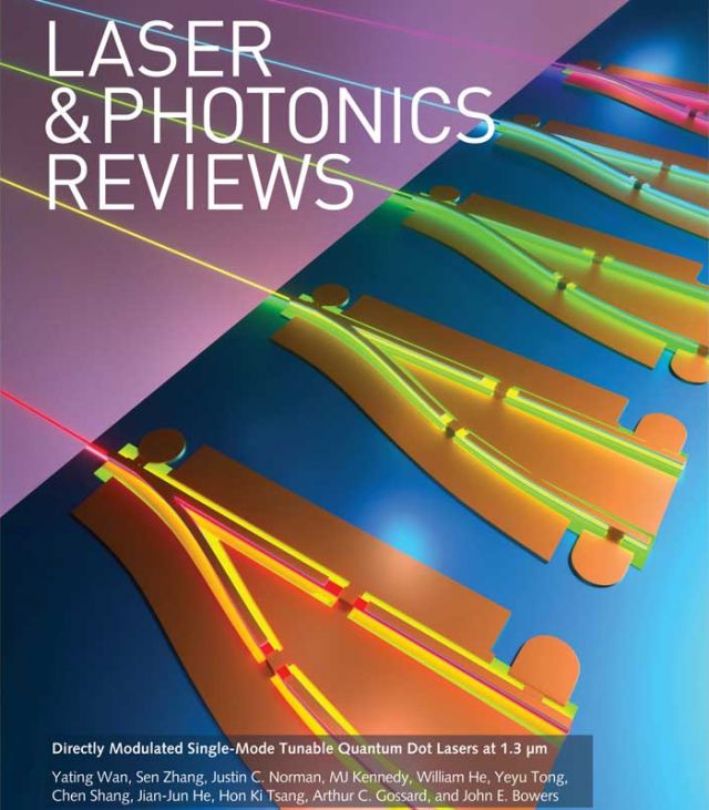
These high capacity transmitters use a lot of integration to achieve tens of Tbps data rates using transistors operating at tens of Gbit/s. Combs of optical frequencies are generated and each wavelength is encoded with data at rates of 25 Gbps today and 100 Gbit/s at the end of the decade. Fig. 1 (see below) shows the level of integration that has been achieved with three dominant technologies: InP photonics, silicon photonics with separate “disaggregated” lasers and silicon photonics with integrated lasers. Silicon is a very inefficient light emitter, so lasers are integrated using direct bandgap III-V materials. This is accomplished by either bonding III-V material to silicon or epitaxially growing the III-V material on silicon. The former was invented at UCSB and is now in commercial production at Intel and two UCSB spinoffs (Aurrion, acquired by Juniper and Nexus Photonics), and the latter is an active area of research at UCSB. It turns out that a new technology, quantum dot lasers, developed in collaboration with Professors Arthur Gossard, Kunal Mukherjee and Jonathan Klamkin, is ideal for highly reliable lasers on silicon and lifetimes have improved over the past decade from hundreds of hours to hundreds of millions of hours. This was accomplished through a detailed study of dislocations and their movement during lasing. The solution is a UCSB invention licensed by a UCSB silicon photonics spinoff, Quintessent.
15 years ago, at UCSB, we started focusing on laser integration hoping to make lasers on silicon as good as lasers on InP or GaAs. Fortunately, ultralow loss silicon nitride waveguides on silicon, developed in collaboration with Professor Dan Blumenthal, allow us to make much better lasers on silicon. By self injection locking DFB lasers to silicon nitride waveguides, the noise of the DFB laser can be reduced by over 40 dB, and the Lorentzian linewidth can be reduced from 1 MHz to 1 Hz, as shown in Fig. 2 (see below). We used to think of semiconductor lasers as noisy, but now they can be lower noise than gas or fiber lasers, and that may open up a lot of new applications for these compact, CMOS capatible, low cost lasers and photonic integrated circuits that use them. Most recently, in collaboration with Professor Galan Moody and the UCSB Quantum Foundry, we are using them for quantum computing applications.

