Palmstrøm "Novel Materials for Next-Gen Devices"
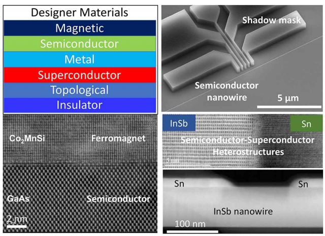
Professor Chris Palmstrøm's group focuses on integrating materials with different electronic and magnetic properties, ranging from semiconducting and insulating to metals and superconductors, in order to create single crystal epitaxial structures to be used in novel devices

Professor Chris Palmstrøm's group focuses on integrating materials with different electronic and magnetic properties, ranging from semiconducting and insulating to metals and superconductors, in order to create single crystal epitaxial structures to be used in novel devices
Novel devices are key to the development of quantum information systems as well as ultra-low power electronics and photonics. These novel devices are made possible by new materials and materials combinations as well as breakthroughs in fabrication. Professor Chris Palmstrøm's group focuses on integrating materials with different electronic and magnetic properties, ranging from semiconducting and insulating to metals and superconductors, in order to create single crystal epitaxial structures to be used in novel devices. These materials are fabricated using multiple molecular beam epitaxial growth systems interconnected by ultra-high vacuum sample transfer in order to grow novel heterostructures of dissimilar materials and characterized at the atomic level without breaking vacuum using scanning tunneling microscopy and electron spectroscopy techniques.
The Potential of Heusler Compounds
Heusler compounds are a class of ternary compounds with cubic crystal structures similar to III-V compound semiconductors. They can be metallic, magnetic, semiconducting, superconducting and topological. These characteristics suggest that Heusler compounds can go beyond the band gap engineering enabled by conventional compound semiconductors to engineer a much wider range of electronic and magnetic properties, thereby creating heterostructures with unique properties. The Palmstrøm group has grown a number of Heusler compounds epitaxially on III-V semiconductors. Through elemental substitution, they have demonstrated the ability to tune the properties from a semiconductor to a ferromagnetic metal.
Some ferromagnetic Heusler compounds have been predicted to have 100% spin polarization of the electrons at the Fermi level. This means that the electrons with majority spin behave as in a metal and the ones with minority (opposite) spin behave as in a semiconductor. Known as half- metals, these compounds are ideally suited for spintronic devices where the performance depends on the spin rather than charge properties of the electron. Heusler-based magnetic tunnel junctions have shown some of the highest magnetoresistance ratios to date with applications in magnetic hard disk read heads and magnetic random access memory devices. Palmstrøm’s group, in collaboration with Paul Crowell’s group at the University of Minnesota, have shown record spin accumulation in GaAs, opening up the possibility of semiconductor-based spintronic devices.
Topological properties are predicted in a number of Heusler compounds, resulting in electronic states with linear energy-momentum dispersion where the electron spin and momentum are locked. Electrons with spins of opposite sign will move in opposite directions, a property that could prove useful for spintronic devices. To enhance the electronic transport properties, Palmstrøm group members Hadass Inbar, Alex Chang, Connor Dempsey, Aaron Engel, Shinichi Nishihaya and Shouvik Chatterjee are working on tuning the electronic structure through elemental substitution and strain. They are also investigating other topological materials that can be grown on III-V semiconductors including rare- earth monopnictides (rare-earth- group-V compounds) that have been predicted to be Dirac and Weyl semimetals.
Read more from this article: Materials for Quantum Information Systems, Novel Semiconductor Devices, The Next Generation
The ECE Current (F20) "Novel Materials for Next Generation Devices" (full article, pg 8)