Nanofab "Uplifting the Local Semiconductor Industry"
For nearly twenty years, the UC Santa Barbara Nanofabrication Facility, better known as the Nanofab, has served as an epicenter for innovation
From the COE News article – "Uplifting the Local Semiconductor Industry"
Nanofab's open-access, shared-use facility features 12,000 square feet of clean room space and houses more than $60 million worth of advanced nanofabrication equipment to enable researchers from academia, industry, and government agencies to bring bold ideas in micro- and nano-technology to life. The Nanofab serves as a cornerstone for both cutting edge research, workforce training at all educational levels, and small-business generation and product commercialization. Technologies developed in the facility have revolutionized numerous industries, ranging from quantum computing and power electronics, to light-emitting diodes (LED) and lasers, to radio frequency (RF) devices and photonic integrated circuits (PICs).
“The devices and fabrication processes that we design here, and the chips that come out of this lab actually solve real-world problems, which is why you see so many companies, from large to small businesses, come to this facility,” said Demis John, the Nanofab’s process group manager.
Operating as a “makerspace” for microchips, the facility welcomes more than 500 users annually, about half of which are from industry, comprising, according to Nanofab management, the country’s largest industrial base supported by a university nanofabrication facility. Since 2006, users from nearly 275 companies nationwide have accessed the Nanofab, three-quarters of which were small businesses, with roughly two-thirds being California-based. Nearly 70 companies that used the facility were based in the Santa Barbara/Goleta area, and almost half of those were founded and/or led by UCSB faculty or alumni. A new grant promises to extend the campus’s ability to serve such innovators.
“Our time-tested and financially sustainable model, which is funded entirely through user fees, allows companies to develop next-generation chip technology at a fraction of the cost required to set up their own facilities,” said UCSB Nanofabrication Facility Director Brian Thibeault. “We provide fast and efficient development due to local control of the resources, which is critical for the high-paced, rapidly advancing semiconductor industry.
As a testament to the university’s strong reputation in the semiconductor industry and the pivotal role the facility plays in the lab-to-fab process of transferring research from the lab to a manufacturing plant, UCSB was selected as a member of the California Defense Ready Electronics and Microdevices Superhub (California DREAMS), a regional innovation hub established by the Department of Defense with funding from the Creating Helpful Incentives to Produce Semiconductors (CHIPS) and Science Act.
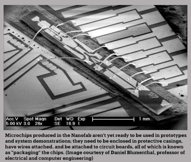
However, chip manufacturing is only one link in the chain of events required to bring viable products to market. Using advanced technology in real-world applications also requires packaging and prototyping. Packaging refers to the process of enclosing the chip in a protective casing while getting electrical or optical signals into the chip, which then enables the technology to be integrated into larger advanced systems. Prototyping involves the creation of early-stage versions of devices, chips or systems to validate designs, test functionality, and identify and resolve issues before mass production. Designing and fabricating a brand-new type of microchip in the Nanofab is a very complex process; however the subsequent packaging and prototyping is an equally complex and critical process. The problem that nearly all Nanofab users face is that the region houses no open-access packaging and prototyping facilities.
“Many companies, especially the smaller businesses that innovate at the Nanofab, are forced to rely on vendors and partners outside of the region to demonstrate packaged prototypes,” explained Demis. “As a result, these companies suffer delays, lose control in the lab-to-fab process, and miss out on the opportunity to further innovate in the prototyping arena.”
The UCSB College of Engineering wants to change that by establishing an open-access advanced prototyping and packaging facility to complete the region’s precision semiconductor manufacturing ecosystem and unlock its full potential. The university’s efforts to meet the regional needs of both researchers and product designers received a major boost from Uplift Central Coast, a six-county partnership that works to advance economic resilience, environmental sustainability, and equitable growth across the region. Uplift, which identified precision manufacturing as one of the region’s key sectors for economic growth, awarded UCSB a $500,000 Catalyst Grant to help make the prototyping and packaging facility a reality. Uplift awarded a total of $9 million to 36 projects out of 136 proposals, providing funding for predevelopment activities such as feasibility studies, site assessments, and early-stage planning, while ensuring that projects are well-positioned for future investment from private, governmental, and philanthropic sources.
“We are extremely grateful to Uplift awarding UCSB the Catalyst Grant and for recognizing the critical role that we play in the regional semiconductor industry,” said Demis. “This funding will expedite our efforts to establish what I believe will be the only open-access prototyping and packaging facility at a university.”
The grant will allow UCSB to hire a technical lead to move the project forward, performing essential duties such as seeking funding to purchase up to $20 million in state-of-the-art prototyping equipment, hire and train professional staff, and finalize the operational business model.
“The facility will serve as an integral component of an oasis in the nation’s desert of lab-to-fab and increase UCSB’s direct support for high-growth entrepreneurship and bolster the semiconductor ecosystem,” said Umesh Mishra, dean of the UCSB College of Engineering. “The project will also ensure that the researchers who use the Nanofab and the new facility stay at the forefront of innovation and contribute to the growth of the semiconductor industry at both the local and national levels.”
John describes the facility as “the missing piece of the research puzzle,” adding that it will eliminate a debilitating pain point to advancements in technology, and that UCSB students and postdoctoral researchers will also benefit greatly from the prototyping facility by becoming experts in packaging and giving them further control of their projects.
“Right now, a lot of research gets stuck at the packaging level for various reasons — the prototyping happens somewhere out of the area, or the students graduate, the funding runs out, or the project goes stagnant,” explained John. “This new facility will eliminate a significant roadblock, and allow researchers to seamlessly transition to the next step in the lab-to-fab process and, ultimately, deliver more impactful technologies to the market.”
The team is currently evaluating possible locations for the new facility and potential funding sources to purchase the equipment.